⚡ PCB
PCB
Printed circuit board
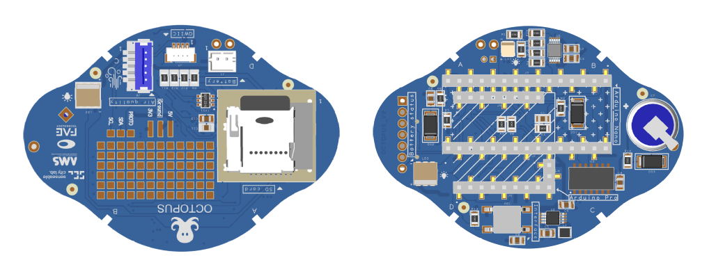
The custom PCB can be set up in two ways:
- Order the PCB from a manufacturing company and ask them to pre-solder the components for you. This is a service often called PCBA (PCB Assembly)
- Order the board and all small hardware components separately, and solder it by hand. Note, this requires you to know how to solder small components.
Files
Gerber files and schematics can be found in the Github repository
Schematics
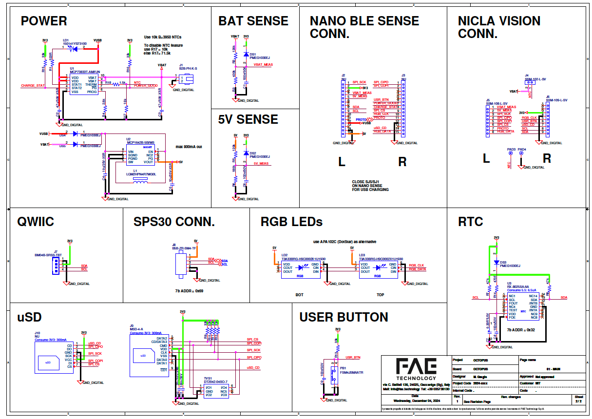
PCB specifications
- BOARD SIZE (XxYxZ): 69.951x50.268x1.6mm
- IPC-6012 - IPC-A-600: CLASS 2
- BOARD TOLERANCE (X|Y|Z): +/-0.2 | +/-0.2 | +/-10%
- E-TESTING: YES
- NO.OF LAYERS: 4
- UL-WARKING: YES
- BASE COPPER OUTSIDE: 18um
- MICROVIA (hole < 100um): NO
- BASE COPPER INSIDE: 35um
- BLIND VIA: NO
- FINISH: ENIG
- BURIED VIA: NO
- SOLDER COLOR: BLUE
- VIA FILL/VIA IN PAD: NO
- SILKSGREEN COLOR: WHITE
- MIN. VIA SIZE: 0.254mm
- DIELECTRIC MATERIAL: FR4-TG150
- MIN.TRACE SPACING: 0.2mm
- IMPEDANCE CONTROL: NO
- QUIER LAYER MIN.TRACE WIDTH: 0.2mm
- CTI: 175V
- INNER LAYER MIN.TRACE WIDTH: 0.2mm